
221 Westmoreland Drive Latrobe, PA 15650 USA
P.O. Box 388 Youngstown, PA 15696-0388 USA
SEM - Scanning Electron Microscope
Scanning Electron Microscope Overview
The Scanning Electron Microscope utilized by Westmoreland Mechanical Testing and Research possess a variety of detectors and functionality designed to allow the user to obtain a variety of information. The detectors currently in use include the Secondary Electron Detector, the Backscattered Electron Detector, and the Energy Dispersive Spectrometer (ASTM 1508).
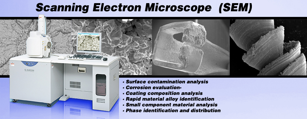 WMTR currently utilizes two SEM units manufactured by Hitachi (3400-N) and Topcon (ABT-6)
SEM/EDS is typically used for:
· Surface contamination analysis
· Corrosion evaluations
· Coating composition analysis
· Rapid material alloy identification
· Small component material analysis
· Phase identification and distribution
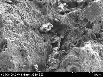
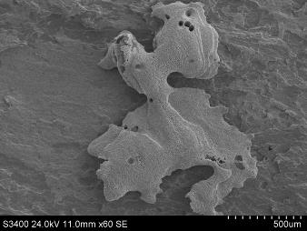
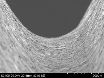
Secondary Electron Detector
The Secondary Electron (SE) Detector allows the operator to view a sample with regards to its basic topographical structure. Similar to light microscopy, electrons from the electron gun hit the sample, and are bounced back to the Secondary Electron Detector. The signals are then analyzed by the microscope and an image may be viewed on the screen. This method of analysis offers a fast and user friendly method of viewing the sample surface in a variety of conditions. Some typical images observed by Secondary Electron Detection are displayed below:
Backscattered Electron Detector
Energy Dispersive Spectrometer (EDS)
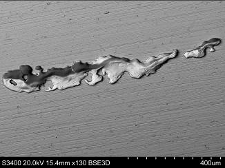
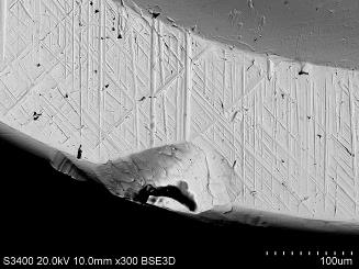
Backscattered Electron Detector
The Backscattered Electron (BSE) Detector implemented by WMTR allows the user to select from a variety of functions inherent to the software. Basic BSE analysis allows the user to view a field a view with regards to the differing atomic masses of atoms present in a given field of view. Elements of a heavier atomic mass which are un-homogenized will show up as a different color than those of a lighter atomic mass. This method is crucial when analyzing a sample for contaminants present when speed is a factor. Coupled with EDS analysis, Compositional BSE analysis offers definitive method of elemental analysis.
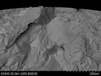
The BSE detector also allows the user to take topographic data one step further. The Detector itself has multiple lobes which, when positioned over the sample, allow the user to gain data from multiple viewpoints. By turning off and on the lobes, the user may view (with greater detail) topographic data of a given sample. The BSE detector also has the capability to capture a 3 Dimensional image, allowing the user to generate a 3D rendering in software, allowing topographic measurements to be taken at any field of view.
One of the largest benefits of BSE analysis is the opportunity for Variable Pressure analysis. SEM/EDS analysis depends greatly upon the tendency of an object to conduct electricity as it is bombarded with electrons from the electron beam. By allowing the SEM to operate at partial pressure (different form the usual Vacuum state), the user may obtain SEM images from a sample which does not conduct electrons as efficiently as a pure metal sample would.
WMTR also has the ability to Gold Plate a sample in order to analyze a non-conductive sample in both SE and BSE modes.
See Also:
Secondary Electron DetectorEnergy Dispersive Spectrometer (EDS)
Energy Dispersive Spectroscopy: ASTM E 1508
At Westmoreland Mechanical Testing & Research ASTM E 1508 is the most commonly employed specification for analysis via Scanning Electron Microscope / Energy Dispersive Spectroscopy.
Energy Dispersive Spectroscopy, or EDS, is a Semi-Quantitative method of analysis which measures the elemental constituents of a sample by analyzing the amount of X-Rays produced versus the energy of such X-Rays when a solid sample is irradiated by an electron beam from a Scanning Electron Microscope. The data collected from such analysis may be very helpful in identifying features or phases in various materials.
When the sample is bombarded by the electron beam of the Scanning Electron Microscope, electrons are ejected from the atoms comprising the sample's surface. A resulting electron vacancy is filled by an electron from a higher energy level, emitting an x-ray of a characteristic wavelength, proportional to the specific energy gap within the atom itself.
The Energy Dispersive Spectrometer’s x-ray detector measures the number of emitted x-rays compared to their energy. The energy of the x-ray is characteristic of the element from which the x-ray was emitted. A spectrum of the energy versus relative counts of the detected x-rays is obtained and evaluated to determine quality and quantity of elements present in the sample.
Elements with atomic numbers from beryllium to uranium can be detected. Depending on the element and matrix, the minimum detection limits vary.
Quantitative results are readily obtained without standards. However, the accuracy of standard-less quantitative analysis is highly dependent on the sample. Greater accuracy is obtained using known standards with similar structure and composition as the unknown sample.
Qualitative observations/measurements may be obtained through a variety of methods. The EDS unit has the capability of mapping elements present on a sample and superimposing a colored “map” of the location and concentration of various elements on top of a captured electron image. The Backscattered Electron Detector may also be used when elements with differing atomic masses are found, un-homogenized, within the same sample. Contamination and corrosion may also be viewed by such a method.
Additional EDS Information Available:
Elemental mapping
Point/Area Analysis
Line profile analysis
Elemental mapping
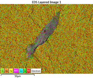
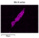
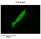
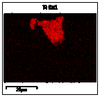
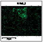
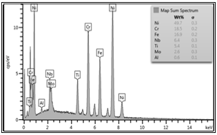
Characteristic x-ray intensity is measured relative to lateral position on the sample surface. Variations in x-ray intensity then indicate the relative elemental concentrations across the surface. Maps are recorded using image brightness intensity as a direct function of the local concentration of the element or elements present. Lateral resolution of about 1µm is possible. EDS elemental mapping allows for all detectable elements to be analyzed at the same time, making a fast analysis possible in a variety of settings.
Example of typical data output/display of elemental mapping is seen in the following images. A spectrum considering the entire field analyzed is also included with the qualitative data. Spectra may also be recreated from a smaller area from the existing map data at a later point in time if required.
Point/Area Analysis
The EDS unit possesses the ability to pin point features within a field of view and gather a spectrum based upon a variety of user demands. The point scan allows the user to concentrate the X-Ray collection on a singular point within a field of view. Multiple point scans may be gathered in quick succession in order to compare gathered data. These collected spectra may then be overlaid onto one another in order to analyze the differing elemental constituents found at various locations. The same type of analysis may be taken of a circular, rectangular, or a user drawn area in order to obtain information from a larger location.
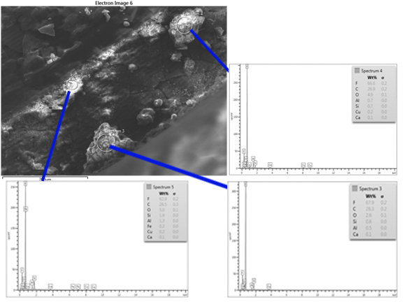
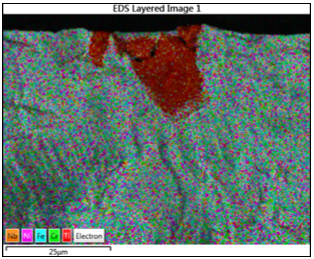
Typical use for such analysis may be to analyze the spectra from an inclusion or contaminant while disregarding the surrounding base metal. Below, an image is observed where the customer had requested the contaminant present on the surface to be analyzed. Three finite area scans were collected on the electron image to characterize a variety of contaminant present.
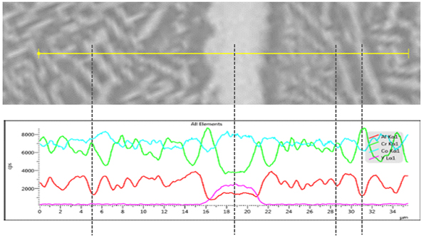
Line profile analysis
The Scanning Electron Microscope's electron beam is scanned along a pre-determined line across the sample while x-rays are detected for specific positions along that line. Analysis of the x-ray energy spectrum at each position provides plots of the relative elemental concentration for each element compared to position along the line. The data may then be displayed by a qualitative graph, showing the increase or decrease of all elemental constituents present at all points on the line. The data may also be condensed into more quantitative data by compressing the data captured along the line into equi-spaced spectra.
A typical example of data displayed from a Line profile analysis is displayed below. The qualitative lines may be displayed “stacked” on the same chart so as to compare relative intensities, or separated onto multiple charts to display the “tiled” form of the data, allowing the relative change of one element to be viewed separately from the rest.
Data collected from the line scan may now also be quantified by “binning” data and set increments along the line. A variety of binning factors may be used to fit the customers explicit need.